
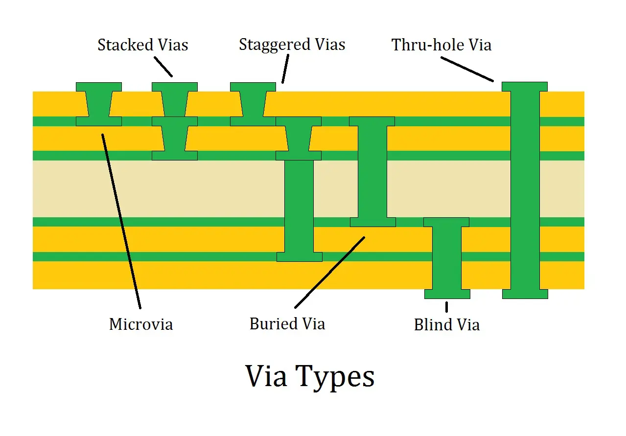
Vias serve as crucial conductive pathways that establish electrical connections between different layers of a Printed Circuit Board (PCB). These pathways, depending on their application, are categorized into through-hole, blind, buried, and microvias. Microvias, in turn, are subdivided into stacked and staggered configurations.
Each via comprises three main elements: a barrel, a pad, and an anti-pad. The barrel, a conductive tube filling the drilled hole, connects via pads to components, planes, or traces. Surrounding the barrel is the anti-pad, providing clearance between the barrel and non-connected metal layers.
Types of PCB Vias
- Through-hole vias: These traverse the entire board from top to bottom, categorized as either plated (PTH) or non-plated (NPTH).
- Blind and buried vias: Blind vias extend from an outer layer to an inner layer, while buried vias link inner layers, enhancing signal integrity and reducing noise and crosstalk.
- Microvias: Laser-drilled with diameters under 150μm, microvias are crucial in High-Density Interconnect (HDI) PCBs, promoting miniaturization and enabling higher routing densities.
Microvias significantly improve electrical characteristics, reduce the need for through-hole vias, and facilitate Breakout of Ball Grid Array (BGA) components. Their ideal aspect ratio of 0.75:1 ensures reliable copper plating within minimal layers, enhancing overall PCB performance.
Benefits of Microvias in HDI Design
Aspect Ratio Considerations
Maintaining an optimal aspect ratio is critical for via reliability. Microvias ideally adhere to a 0.75:1 ratio, while through-hole vias typically aim for 10:1. Exceeding these ratios can escalate design complexity and reliability concerns.
Integration of Via-in-Pad
To accommodate high signal speeds and dense component layouts, Via-in-Pad (VIP) configurations are utilized. These vias streamline thermal management, reduce space requirements, and simplify BGA routing, ensuring robust signal integrity.
PCB Design Guidelines
When implementing vias using Electronic Design Automation (EDA) tools, adherence to design rules and utilizing advanced features like automated routing and design rule checks (DRC) is crucial. Staggered vias are preferred over stacked alternatives to mitigate planarization complexities and reduce manufacturing costs.
Conclusion
Effective via design is pivotal in optimizing PCB performance and reliability. Designers must master via integration techniques to achieve superior routing strategies and ensure seamless board functionality.
integration techniques to achieve superior routing strategies and ensure seamless board functionality.