PCB

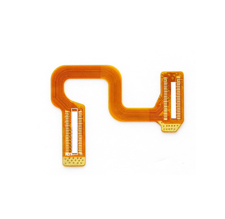
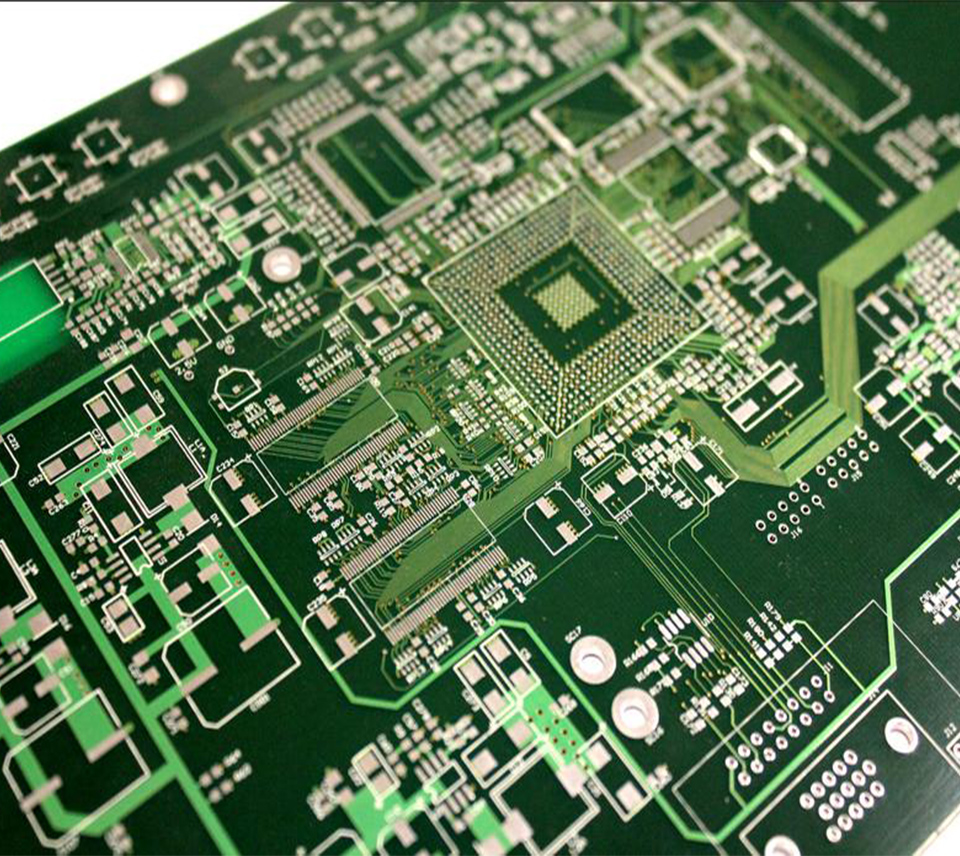
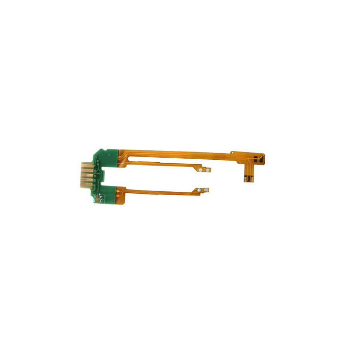
PCB know as Printed Circuit Board, or PWB, a pcb is mechanically support electronic components using conductive pads in the shape designed to accept the component’s terminals, and also electrically connect them using traces, planes and other features etched from one or more sheet layers of copper laminated onto and/or between sheet layers of a non-conductive substrate. Components are generally soldered onto the PCB to both electrically connect and mechanically fasten them to it. PCBs can be single-sided, double-sided, or multi-layer, or Rigid Flex.
WHAT CAN WE DO FOR PCB?
Material:PI : 3mil 2mil 1mil 0.8mil 0.5mil
ED&RA Cu : 2OZ 1OZ 1 / 2OZ 1 / 3OZ 1 / 4OZ
Shengyi / Taiflex / Dupont / Doosan / Thinflex
Flex PCB capability:1-10 Layers
Min. Thickness:0.08 +/- 0.03mm
Max. Thickness:6mm
Max. Size:485mm * 1000mm
Min.Hole:0.15mm
Min.Slot Hole:0.6mm
Aspect Ratio: 10-1
Min.Width / Space: 0.05 / 0.05mm


Material:
FR-4(High Tg, Halogen Free, High Frequency)
FR-5, CEM-3, PTFE, BT, Getek, Aluminium base,Copper base,KB, Nanya, Shengyi, ITEQ, ILM, Isola, Nelco, Rogers, Arlon
Finishing:
HASL
Lead Free HASL
Immersion Gold (ENIG), Immersion Tin, Immersion Silver
Organic Solderability Preservative (OSP) / ENTEK
Flash Gold(Hard Gold plating)
ENEPIG
Selective Gold Plating, Gold thickness up to 3um(120u”)
Gold Finger, Carbon Print, Peelable S/M
Material:PI : 3mil 2mil 1mil 0.8mil 0.5mil
ED&RA Cu : 2OZ 1OZ 1 / 2OZ 1 / 3OZ 1 / 4OZ
Shengyi / Taiflex / Dupont / Doosan / Thinflex
Flex PCB capability:1-10 Layers
Min. Thickness:0.08 +/- 0.03mm
Max. Thickness:6mm
Max. Size:485mm * 1000mm
Min.Hole:0.15mm
Min.Slot Hole:0.6mm
Aspect Ratio: 10-1
Min.Width / Space: 0.05 / 0.05mm

GET IN TOUCH