When it comes to Surface Mount Technology (SMT) production, cases of welding failure caused by missing drill files are not uncommon.
Solder paste printing in SMT welding is a crucial and rather complex process, with data suggesting that 60-70% of defects in SMT production stem from solder paste printing.
Interestingly, these defects are not equipment-related but primarily emerge during engineering assessments and stencil optimizations. In particular, the absence of drilling files during engineering can lead to various SMT welding defects.
According to data provided by Company E’s Engineering Department at major welding factories, about 15% of SMT welding cases lack drilling layer files. This omission leads to at least one or more daily orders where customers fail to provide these essential files. It incurs significant communication costs, estimated at around 100 minutes per day and over 43 hours per month, arising from email exchanges between engineers, PMC, and customers to confirm and fulfill these requirements.
The stencil plays a pivotal role in SMT welding and requires a systematic approach beyond simple hole drilling. Understanding how to prevent tin ingress causing soldering issues, the necessity of drilling layer files for stencil design, and addressing various real-world cases are crucial.
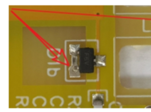
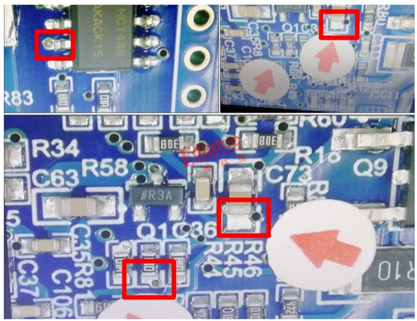
- For instance, issues arise when edge holes on solder pads aren’t identified due to the absence of drilling files. The consequence: unsatisfactory soldering, false soldering, and inadequate tin in resistors or connectors.

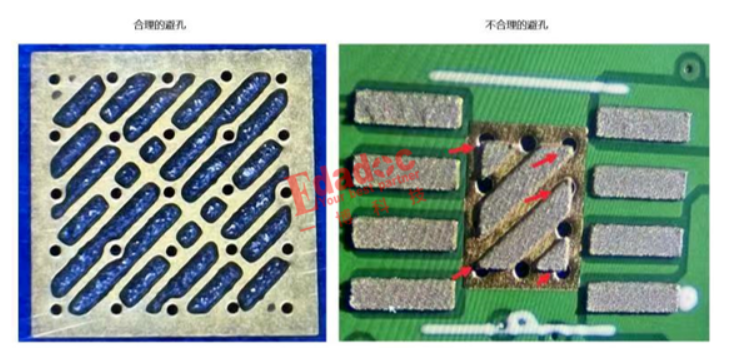
Similarly, the lack of avoidance holes in QFN ground solder pads results in tin ingress and false soldering. Here, it’s vital to avoid or increase tin filling in the holes to ensure sufficient coverage. Failure to provide drilling layer files prevents timely detection and avoidance of such problems during stencil creation.

Furthermore, the rush to create stencils without physical inspection of the PCB bare board can lead to issues. When customers fail to provide drilling layer files, issues such as unanticipated plate-through holes can arise during stencil creation, leading to welding anomalies.
To mitigate these concerns, it’s essential to evaluate plate-through holes for chips, maintain a distance between through-holes and SMDs, and understand the importance of resin plug-hole electroplating processes in PCBa design.

In summary, by avoiding plate-through holes and ensuring the provision of drilling layer files for stencil design, welding quality can be significantly improved. This not only aids in precise hole identification but also prevents unnecessary or insufficient holes, thereby averting potential quality hazards due to poor design choices.