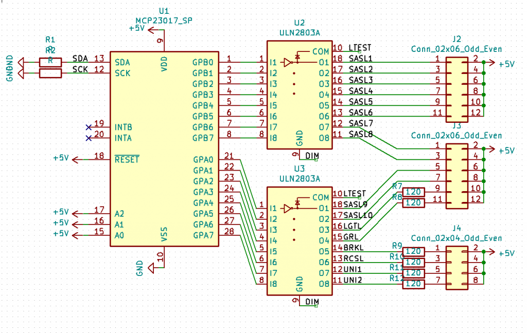
A schematic diagram is a fundamental two-dimensional representation showing the functionality and connectivity between different electrical components. It is crucial for PCB designers to familiarize themselves with schematic symbols that represent these components.

Standards for Schematic Symbols
Schematic symbols are standardized globally using two main standards:
- IEC 60617: Issued by the International Electrotechnical Commission (IEC), based on the older British Standard (BS 3939). It includes over 1750 schematic symbols.
- ANSI Y32: Issued by the American National Standards Institute (ANSI), originally for aircraft applications, now aligned with IEC through minor revisions.
Common Schematic Symbols
A schematic diagram uses standardized symbols to represent various electronic components, such as resistors, capacitors, and LEDs. Each symbol has specific attributes, like resistance value for resistors or voltage rating for batteries, which help identify the components and their roles in the circuit.
Values and Attributes
Components are identified by reference designators (e.g., R1 for a resistor) and attributes (e.g., resistance in ohms). It’s essential to include these details to ensure the correct components are used. For instance, capacitors are specified by capacitance (farads), and inductors by inductance (Henrys).
International System of Units (SI)
To simplify circuit diagrams, the International System of Units (SI) is used. For example, large values like 1,000,000 ohms are written as 1MΩ, and small values like 0.000001 farads as 1µF.
Schematic vs. Wiring Diagrams
Schematic Diagram: Uses symbols and lines to show connections and functionality, without detailing physical layout.
Wiring Diagram: Provides a pictorial representation with simplified shapes and detailed information about component locations and arrangements.
Reading a PCB Schematic
A PCB schematic provides information on components, electrical connections, operating conditions, and special instructions. It includes schematic nets (lines connecting components), junctions (intersections of wires), and nodes (dots at intersections indicating connections).
Naming Schematic Nets
Nets in a schematic are labeled for clarity. Nets with the same name are assumed to be connected, even if no visible connection is shown. This labeling helps in understanding the circuit’s connectivity.
Schematic Diagram vs. PCB Layout
Schematic Diagram: Shows logical connections and includes a netlist, listing every connection in the design.
PCB Layout: Shows physical locations of components and the traces connecting them.
Creating a Schematic Diagram
Steps to create a schematic diagram using PCB CAD tools include:
Symbol Generation: Draw component symbols, add pins and attributes, and assign footprints.
Component Placement: Place symbols on the schematic, ensuring proper pin numbering and attribute assignment.
Rules for Drawing Schematic Diagrams
Follow these best practices:
- Use lines to represent electrical connections; add nodes at intersections for connections.
- Assign names to nets in complex circuits.
- Write pin numbers, values, and net names horizontally.
- Place inputs on the left and outputs on the right.
- Design sections in functional blocks.
- Place pin numbers outside the symbol graphic.
- Position sheet connection symbols on the extreme left or right edges.
- Include a title block with the title, part number, and revision on the lower right corner of the first sheet.
Understanding schematic diagrams is essential for designing successful PCBs. They consist of component symbols and lines representing connections, helping designers visualize and plan their circuits effectively.